加载头像

FCC E6A - 电路元件与半导体

FCC 题库总览 > E级 (最高特级 Extra) > E6 电路元件与半导体 > E6A

小节 E6A:电路元件与半导体

本小节共包含 12 道中英双语精校考题
#E6A01🔗
In what application is gallium arsenide used as a semiconductor material?
砷化镓作为半导体材料有哪些应用?
A
In high-current rectifier circuits
在大电流整流电路中
B
In high-power audio circuits
在大功率音频电路中
C
In microwave circuits
在微波电路中
✓ 正确答案
D
In very low-frequency RF circuits
在极低频射频电路中
#E6A02🔗
Which of the following semiconductor materials contains excess free electrons?
以下哪种半导体材料含有多余的自由电子?
A
N-type
N型
✓ 正确答案
B
P-type
P型
C
Bipolar
双极性
D
Insulated gate
绝缘栅
#E6A03🔗
Why does a PN-junction diode not conduct current when reverse biased?
为什么 PN 结二极管反向偏置时不导通电流?
A
Only P-type semiconductor material can conduct current
只有P型半导体材料才能导电
B
Only N-type semiconductor material can conduct current
只有N型半导体材料才能导电
C
Holes in P-type material and electrons in the N-type material are separated by the applied voltage , widening the depletion region
P型材料中的空穴和N型材料中的电子被施加的电压分开,加宽了耗尽区
✓ 正确答案
D
Excess holes in P-type material combine with the electrons in N-type material, converting the entire diode into an insulator
P型材料中多余的空穴与N型材料中的电子结合,将整个二极管转变为绝缘体
#E6A04🔗
What is the name given to an impurity atom that adds holes to a semiconductor crystal structure?
在半导体晶体结构中添加空穴的杂质原子叫什么名字?
A
Insulator impurity
绝缘体杂质
B
N-type impurity
N型杂质
C
Acceptor impurity
受主杂质
✓ 正确答案
D
Donor impurity
供体杂质
#E6A05🔗
How does DC input impedance at the gate of a field-effect transistor (FET) compare with that of a bipolar transistor?
场效应晶体管 (FET) 栅极的直流输入阻抗与双极晶体管的直流输入阻抗相比如何?
A
They are both low impedance
它们都是低阻抗
B
An FET has lower input impedance
FET 具有较低的输入阻抗
C
An FET has higher input impedance
FET 具有更高的输入阻抗
✓ 正确答案
D
They are both high impedance
它们都是高阻抗
#E6A06🔗
What is the beta of a bipolar junction transistor?
双极结型晶体管的贝塔值是多少?
A
The frequency at which the current gain is reduced to 0.707
电流增益降低至 0.707 时的频率
B
The change in collector current with respect to the change in base current
集电极电流的变化相对于基极电流的变化
✓ 正确答案
C
The breakdown voltage of the base-to-collector junction
基极-集电极结的击穿电压
D
The switching speed
开关速度
#E6A07🔗
Which of the following indicates that a silicon NPN junction transistor is biased on?
以下哪项表明硅 NPN 结晶体管处于偏置状态?
A
Base-to-emitter resistance of approximately 6 ohms to 7 ohms
基极至发射极电阻约为 6 欧姆至 7 欧姆
B
Base-to-emitter resistance of approximately 0.6 ohms to 0.7 ohms
基极至发射极电阻约为 0.6 欧姆至 0.7 欧姆
C
Base-to-emitter voltage of approximately 6 volts to 7 volts
基极至发射极电压约为 6 伏至 7 伏
D
Base-to-emitter voltage of approximately 0.6 volts to 0.7 volts
基极至发射极电压约为 0.6 伏至 0.7 伏
✓ 正确答案
#E6A08🔗
What is the term for the frequency at which the grounded-base current gain of a bipolar junction transistor has decreased to 0.7 of the gain obtainable at 1 kHz?
双极结型晶体管的接地基极电流增益降至 1 kHz 时增益的 0.7 时的频率术语是什么?
A
Corner frequency
转角频率
B
Alpha rejection frequency
阿尔法抑制频率
C
Beta cutoff frequency
贝塔截止频率
D
Alpha cutoff frequency
阿尔法截止频率
✓ 正确答案
#E6A09🔗
What is a depletion-mode field-effect transistor (FET)?
什么是耗尽型场效应晶体管 (FET)?
A
An FET that exhibits a current flow between source and drain when no gate voltage is applied
当未施加栅极电压时,在源极和漏极之间呈现电流的 FET
✓ 正确答案
B
An FET that has no current flow between source and drain when no gate voltage is applied
当没有施加栅极电压时,源极和漏极之间没有电流流动的 FET
C
An FET that exhibits very high electron mobility due to a lack of holes in the N-type material
由于 N 型材料中缺乏空穴,FET 表现出非常高的电子迁移率
D
An FET for which holes are the majority carriers
空穴为多数载流子的 FET
#E6A10🔗
In Figure E6-1, which is the schematic symbol for an N-channel dual-gate MOSFET?
在图 E6-1中,哪个是N沟道双栅极MOSFET的原理图符号?
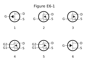
Figure for E6A10
A
2
2
B
4
4
✓ 正确答案
C
5
5
D
6
6
#E6A11🔗
In Figure E6-1, which is the schematic symbol for a P-channel junction FET?
在图 E6-1 中,哪个是 P 沟道结型 FET 的原理图符号?
Figure for E6A11
A
1
1
✓ 正确答案
B
2
2
C
3
3
D
6
6
#E6A12🔗
What is the purpose of connecting Zener diodes between a MOSFET gate and its source or drain?
在 MOSFET 栅极与其源极或漏极之间连接齐纳二极管的目的是什么?
A
To provide a voltage reference for the correct amount of reverse-bias gate voltage
为正确的反向偏置栅极电压提供电压参考
B
To protect the substrate from excessive voltages
保护基板免受过高电压的影响
C
To keep the gate voltage within specifications and prevent the device from overheating
将栅极电压保持在规格范围内并防止器件过热
D
To protect the gate from static damage
保护门免受静电损坏
✓ 正确答案
引用到评论
随便逛逛博客分类文章标签
复制地址关闭热评深色模式轉為繁體